This post follows Designing a step-down converter - part 1.
Board Layout
After finishing designing the schematics, I started doing the layout based on the recommended layout found in the MCP16311 datasheet (Figure 5-1). The result is a simple 2-layer board with both step-down converters next to each other. Everything is routed on the top layer and both top and bottom layers are filled with a ground plane. Block terminals are present to connect input and output wires.
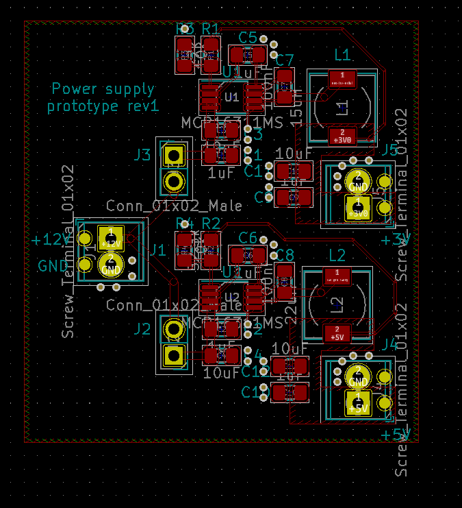
Note that jumpers J2 and J3 are not strictly needed but present nonetheless to make it easier to measure the current consumption with a multi-meter. This will become handy when measuring the efficiency of each step-down converter.
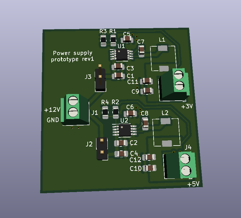
And here is how it looks like on Kicad 3D viewer:
Here are the Kicad files (compatible with Kicad 5).
Building the board
Here is the BOM:
| Name | Reference | Mouser part number | Quantity |
|---|---|---|---|
| MCP16311 | U1, U2 | 579-MCP16311-E/MS | 2 |
| Block terminals | J1, J4, J5 | 651-1725656 | 3 |
| Capacitor 100nF | C7, C8 | 80-C0805C104M3R | 2 |
| Capacitor 1uF | C1, C2, C5, C6, C9, C10 | 710-885012207078 | 6 |
| Capacitor 10uF | C3, C4, C11, C12 | 187-CL21A106KAYNNNE | 4 |
| Resistor 53K | R2 | 71-CRCW080552K3FKEA | 1 |
| Resistor 27K | R1 | 71-CRCW0805-27K-E3 | 1 |
| Resistor 10K | R3, R4 | 71-CRCW080510K0FKEC | 2 |
| Inductor 15uH | L1 | 994-MSS7341T-153MLB | 1 |
| Inductor 22uH | L2 | 871-B82462G4223M | 1 |
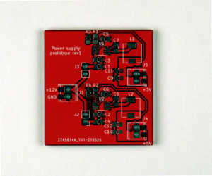
Gerber files were sent to JLCPCB for manufacturing. I also ordered a stencil mask.
And a few weeks later…
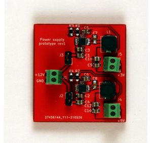
For soldering the components, I used a different method than usual (i.e. soldering everything with a soldering iron). This time, it involved solder paste and a hot air gun.
- I used the solder mask to place solder paste only on the pads of the board.
- I placed all components on the board using some tweezers.
- I used a hot air gun to heat the board and meld the solder paste.
Usually a oven is used instead of a hot air gun, but it did not prevent me from having a good result. Most components aligned well with the pads. It did fail twice because the pads were not heated at the same time. For those two components, I used the soldering iron. Finally, I soldered the block terminals.
And voilà:
Efficiency
To find out the efficiency of each step-down converter, I connected the output of the converter to a bunch of 33, 47 or 68 Ohm resistors. The circuit was powered by a 12V power supply with a 1A current limit. I measured the input current by connecting the multimeter leads on J2 or J3. I also measured the output current, the current going through the resistors.
The formula for computing the efficiency is quite simple:
$$efficiency = \frac{Power_{input}}{Power_{output}} = \frac{voltage_{input} * current_{input}}{voltage_{output} * current_{output}}$$
3V rail
For the 3V rail, I am only concerned about the efficiency when the current is in range 10-100mA.
| Input current (mA) | Output current (mA) | Efficiency (%) |
|---|---|---|
| 6.4 | 18.6 | 73.2 |
| 12.6 | 38.3 | 76 |
| 18.9 | 55.6 | 73.5 |
| 24.8 | 71.9 | 72 |
| 31.9 | 89.7 | 70.3 |
| 39.6 | 108.7 | 68.6 |
| 52.4 | 135.5 | 64.6 |
Overall, I am a bit disappointed about the efficiency of the 3V rail at small loads. Based on the efficiency curve found in the datasheet, I was expecting roughly 80% efficiency. Still, this is much better.
5V rail
For the 5V rail, I have to test the circuit with higher loads, up to 1A.
| Input current (mA) | Output current (mA) | Efficiency (%) |
|---|---|---|
| 34.5 | 64.4 | 77.7 |
| 49.5 | 92.9 | 78.2 |
| 64.7 | 119.6 | 77 |
| 68.3 | 123.8 | 75.5 |
| 83.3 | 144.9 | 72.5 |
Unfortunately, the multimeter readings are coarser above 200mA.
| Input current (A) | Output current (A) | Efficiency (%) |
|---|---|---|
| 0.1 | 0.21 | 87.5 |
| 0.14 | 0.32 | 95.2 |
| 0.19 | 0.42 | 92.1 |
| 0.27 | 0.60 | 92.6 |
| 0.35 | 0.75 | 89.3 |
| 0.38 | 0.83 | 91.0 |
| 0.43 | 0.90 | 87.2 |
The 5V rail is performing as expected.